The original BITX was published on the Internet in the year 2003. In the last 13 years, it has grown to become one of the most popular rigs among radio amateurs around the world. The BITX40 board is this very classic now available as a fully tested board that is easy to hookup, modify and operate. You can read the original article that described the BITX at http://phonestack.com/farhan/bitx.html.
Download the circuit diagrams »
What’s special about this version of the BITX?
- Uses a 12 MHz IF and a Si5351 at 5 MHz as a rock solid local oscillator
- The entire transceiver fits into a single large and easily accessible PCB
- Though it works on 40 meters, it is easy to change coils and work it on other bands (details to be released soon)
- It has a separate power line for the PA. By increasing the PA power voltage, the transmit power can be increased
- The components supplied with the board will get you up on air without any special skill
- Read the Wire Up to understand how it is hooked up
Development Notes
Almost all modes of radio communications share a natural principle that the receivers and transmitters use the same line-up of circuit blocks except that the signal direction is reversed. The CW direct conversion transceiver is the simplest illustration of this principle. A more complex example is the bidirectional SSB transceiver.
Bi-directional SSB transceivers have been quite common in amateur literature. A transceiver was described in the ARRL SSB Handbook using bipolar transistors. W7UDM’s design of bidirectional amplifier (as the basis of bidirectional transceiver) is referred to by Hayward and DeMaw in their book Solid State Design. The bidirectional circuitry is often complex and not approachable by the experimenter with modest capability.
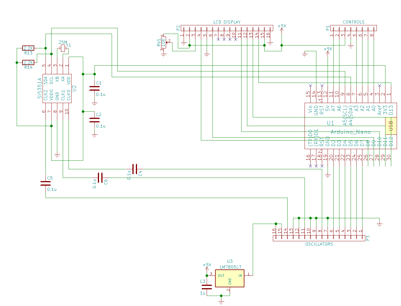
The Raduino
The Raduino is a very powerful, hackable, easy to program board that comes loaded with the BITX40 software. The lower side OSCILLATORS connector has 16 pins. A 5 pin header that sits on it takes 12v, ground, and also provides the DDS output to be connected to the main board’s DDS connector. An 8 pin CONTROLS connector on the top connects to the tuning pot and future switches and controls. The tuning system is very precise and easy. The tuning pot covers 50 KHz of the band and the edge of the tuning pot’s range allow you to scan up and down the rest of the band in 10 KHz steps.
The broad band bi-directional amplifier
My interest in bidirectional transceivers arose after looking at an RC coupled bidirectional amplifier in the book Experimental Methods in RF Design (p. 6.61). An easily analyzed circuit that was simple and robust was required. It began its life as an ordinary broad-band amplifier:
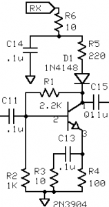
There are some interesting things about this circuit:
- The power gain, and the input and output impedances are all related to the resistor values and do not depend upon individual transistor characteristics. We only assume that the transistor gain is sufficiently high throughout the frequencies of our interest. The precise value of the transistor characteristics will only limit the upper frequency of usable bandwidth of such an amplifier. This is a useful property and it means that we can substitute one transistor for another. You can use 2N3904, BC547, 2N2222, etc. Just about any transistor will do!
- The power gain is not a function of a particular transistor type. We use much lower gain than possible if the transistor was running flat out. But the gain is controlled at all frequencies for this amplifier. This means that this amplifier will be unconditionally stable (it won’t exhibit unusual gain at difference frequencies).
In order to make bidirectional amplifiers, we strap two such amplifiers together, back to back. By applying power to either of amplifiers, we can control the direction of amplification. This is the topology used in the signal chain of this transceiver. The diodes in the collectors prevent the switched-off transistor’s collector resistor (220 ohms) from loading the input of the other transistor. A close look will reveal that the AC feedback resistance consists of two 2.2K resistors in parallel, bringing the effective feedback resistance to 1.1K. All stages of amplification in this transceiver work this principle.
Diode mixers
The diode mixers are inherently broadband and bidirectional in nature. This is good and bad. It is good because the design is non-critical and putting 8 turns or 20 turns on the mixer transformer will not make much of a difference to the performance except at the edges of the entire spectrum of operation.
The badness is a little tougher to explain. Imagine that the output of a hypothetical mixer is being fed to the next stage that is not properly tuned to the output frequency. In such a case, the output of the mixer cannot be transferred to the next stage and it reflects back into the mixer. Ordinarily, if the mixer was a FET or a bipolar device, this reflected power just heats up the output coils. In case of diode ring mixers, you should remember that these devices are capable of taking input and outputs from any port (and these inputs and outputs can be from a large piece of HF spectrum), hence the mixer output at non-IF frequencies reflects back in the mixer and mixes up once more creating a terrible mess in terms of generating whistles, weird signals and distorting the original signal by stamping all over it.
A simple LC band pass filter that immediately follows the diode ring mixer will do a good job only at the frequencies it is tuned to. At other frequencies, it will offer reactive impedance that can cause the above mentioned problems. It is a requirement that the diode mixer’s input and output ports see the required 50 ohms termination at all the frequencies. In other words, they require proper broadband termination. Using broad-band amplifiers is a good and modest way of ensuring that. A diplexer and a hybrid coupling network is a better way, but it would be too complex for this design.
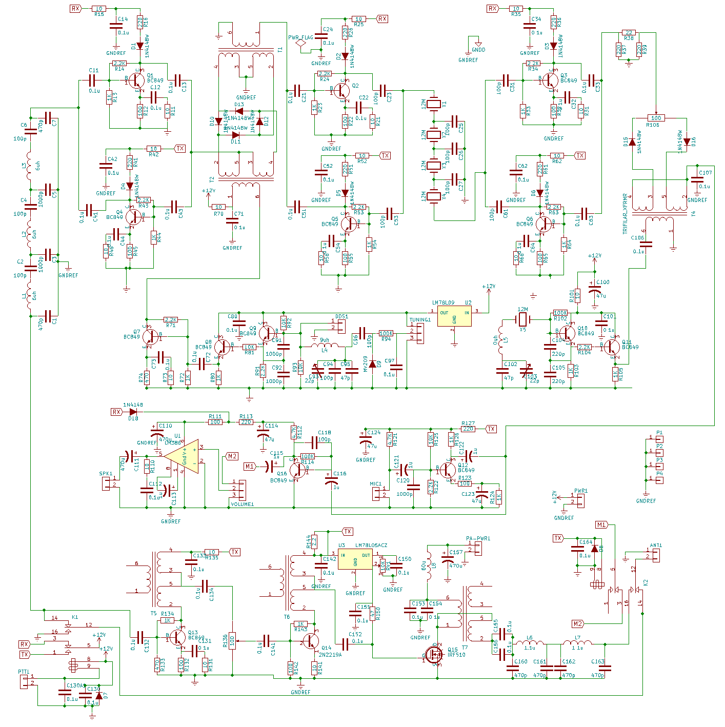
Circuit Description
Although simple, every effort was made to coax as much performance as was possible given the limitations of keeping the circuit simple and affordable.
The Receiver
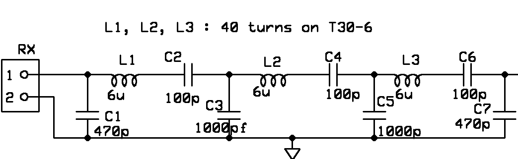
The RF front-end uses a high performance 3 section band-pass filter for strong image and IF rejection. The three poles of filtering provide for a no-tune bandpass filter that needs no adjustment.
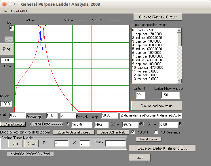
The 7 MHz bandpass filter. Each vertical division is 5 MHzThe RF Amps
An RF amplifier follows the RF band pass filter (Q1). There is 8mAs through the RF amplifier and the post-mix amplifiers to keep the signal handling capacity of the circuit above average. The Post-mix amplifier (Q2) does the job of keeping the crystal filter as well as the diode mixer properly terminated. The crispness of the receiver is more due to this stage than anything else. An improper post-mix amplifier easily degrades the crystal filter’s shape and introduces spurious signals and whistles from the diode mixer.
The Optional VCO
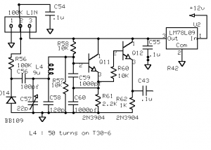
The BITX40 is supplied with the Raduino to make drift free, precise tuning easy. For the purists, a voltage controlled oscillator that covers 4.8 Mhz to 5 Mhz to cover the 7.0 Mhz to 7.2 MHz is an alternative. Just plug out the Raduino and solder the supplied yellow VFO coil. A varactor was chosen over a variable capacitor as it is easier to tune. Mounting a VFO capacitor properly is difficult. Good quality tuning capacitors are nolonger available. Those who like slower tuning rates with the VCO could use a multiturn 10K linear pot instead of a regular potentiometer. The VCO is fed via a broad-band amplifier into the doubly balanced mixer. The trimmer provides exact band covereage. This oscillator has low noise though it does drift a little like all analog oscillators. It settles down to a very imperceptible drift within 10 minutes of warm up. Tip: Turn the BITX40 on for a few minutes before actual use to avoid the warm up drift. The receiver withe the VCO takes just 90 mA current.
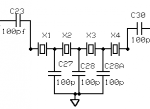
The Crystal filter
BFO, Detector and Audio
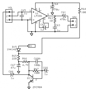
The BFO is a plain RC coupled crystal oscillator with an emitter follower. The emitter follower has been biased to 6V to prevent limiting. The detector also doubles up as the modulator during transmit mode; hence it is properly terminated with an attenuator pad. It has no impact on the overall noise figure as there is enough gain before the detector. The Q13 audio pre-amplifier is a single stage audio amplifier. The 100pf capacitor across the base and collector provides for low frequency response. The receiver does not have an AGC. This is not a major short-coming. Manual gain control allows you to control the noise floor of the receiver and I personally find it very useful when searching for weak signals or turning it down to enjoy the local ragchew.
Transmitter
The microphone amplifier has a DC bias for the mic. This is required for the electret microphone that is supplied with the kit. The common Personal Computer type of headset too need this bias voltage. If your microphone does not require any bias, then insert a 1uF in series with the microphone. The microphone amplifier is a simple single stage audio amplifier. It does not have any band pass shaping components as the SSB filter ahead will take care of it all. One 0.001uf at the microphone input and another at the modulator output provide bypass for any stray RF pickup.
The two diode balanced modulator has a simple balance control. The attenuator pad at the output was found necessary to properly terminate the diode modulator and keep the carrier leakage around the IF amplifier to a minimum.
Rest of the transmission circuitry is exactly the same as the receiver. There is an extra stage of amplification (Q13) to boost the very low level 7 MHz SSB signal from output of the bandpass filter to 1V level : enough to directly drive a driver stage.
Inductor data
The inductors used on the board as follows:
- L1, L2, L3 : 6uh, 40 turns on T30-6 core
- L4 : Only needed the analog VFO, 9uh, 50 turns on T30-6 core
- L5 : just a jumper on the standard bitx40, you will have to an inductor of a few uh to pull the BFO down for upper-sideband
- L6, L7 : 1.1 uh, 17 turns on T30-6 core
- L8 : 10 turns on FT37-43
- T1,T2,T4,T5,T6,T7 : 10 turns trifilar on FT 37-43 core
The L1,L2,L3,L4 need a wire gauge thin enough for the large number of turns. We use 36swg enamelled copper wire, you can use thinner wire if you have any. The rest of the transformers and inductors have use 28 swg.
Note: The L4 is not required with the Raduino or any other digital VFO. The L5 is needed only if you want to operate USB (to pull the BFO to the lower slope of the crystal filter).
Getting Help
Join the mailing list for BITX on https://groups.yahoo.com/group/BITX20/ for all the help you need. You can ask all your questions, get suggestions and help with your BITX project within hours from the mailing list. See you on the band soon!